[email protected]
Professor of Electrical Engineering, University of Tennessee, Knoxville
Research focus: Synthesis and manipulation of 2D materials and other emerging electronic materials, with an emphasis on interface interactions with substrates and surroundings; novel applications of these materials and their properties
Website https://web.eecs.utk.edu/~ggu1/
Bio
Gong joined the Min H. Kao Department of Electrical Engineering and Computer Science at UTK in 2010 to explore the more fundamental aspects of emerging electronic materials, after venturing into the world of 2D materials while working at Sarnoff Corporation in Princeton, NJ. He received his PhD degree in Electrical Engineering in 1999 from Princeton University, where his research was on organic semiconductor devices. Gong is an undergraduate alumnus of the Department of Electronic Engineering of Tsinghua University.
Research Description
The Gu group works at the interdisciplinary junction connecting electrical engineering, physics, and materials science. They synthesize 2D materials (or simply peel them off van der Waals layered crystals), explore their exotic behaviors, and come up with novel applications. With two surfaces but not much of a bulk, a 2D material usually loses its intrinsic properties if not in stringently controlled conditions, hindering experimentation, let alone applications. To this end, the group explores ways to retain the desired intrinsic properties of these atomically thin sheets or to leverage their interactions with the surroundings. In these endeavors, Gong has found the chemical bonding picture of solids useful and become interested in bridging the complementary chemical and physical pictures.
Recent research
https://doi.org/10.1002/anie.202007244 (see also http://science.sciencemag.org/content/369/6499/46.7)
https://pubs.rsc.org/en/content/articlelanding/2020/SC/D0SC00292E
https://pubs.rsc.org/en/content/articlelanding/2016/cp/c6cp01572g
http://www.pnas.org/content/111/47/16670.abstract
http://www.sciencemag.org/content/343/6167/163
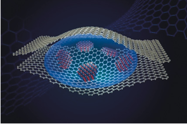
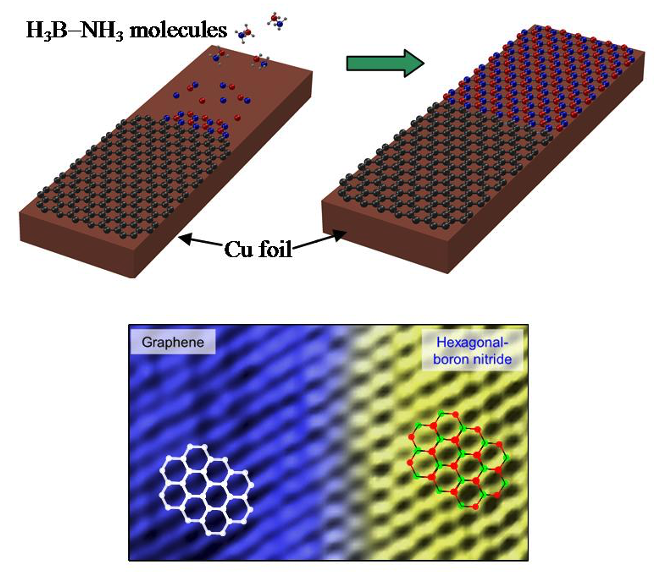
Research Image